Intel and ASML Report More Than One Million High-NA EUV Wafers Processed
The readiness milestone places process integration, metrology, masks and design enablement at the center of next-generation manufacturing intelligence.
Executive summary
What happened—and why it matters
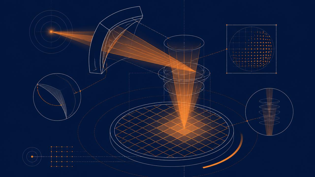
Intel and ASML announced that more than one million wafers had been processed on High-NA EUV systems across certification, R&D and selected production work. The announcement is a manufacturing-readiness milestone rather than a patent event. Its IP value lies in the process, equipment, mask, metrology and integration innovations that can accumulate around deployment.
What happened
The verified development
Intel and ASML announced the milestone on September 7, 2026.
Intel said the volume included tool certification, research and development, and selected Intel 18A production layers.
The announcement did not provide product-level yield or output figures.
Technology signal
High-NA EUV readiness depends on a connected stack of optics, masks, resists, metrology, process control and design rules.
Business implication
Manufacturing learning at scale can shape foundry readiness, customer confidence and defensible process know-how.
IP signal
The portfolio area to monitor
High-volume learning may generate patentable process improvements while also creating valuable confidential know-how. Intelligence work should distinguish equipment-vendor patents, foundry process patents, customer design-enablement assets and trade-secret implementation knowledge.
Why this matters for IP teams
- Map High-NA process patent families
- Monitor mask and metrology claims
- Track Intel–ASML ecosystem filings
- Compare patent and know-how boundaries
- Assess design-enablement dependencies
Competitive landscape
Players and adjacent technologies
Players to monitor
- Intel
- ASML
- Foundries
- Materials and metrology suppliers
Related technologies
- EUV masks
- Photoresists
- Overlay metrology
- Process control
- Advanced nodes
Competitive positioning should be assessed through portfolio-level analysis rather than market-share assumptions.
Monitoring agenda
IP signals to watch
- 01
High-NA process windows
- 02
Large-mask architectures
- 03
Metrology and inspection
- 04
Resist materials
- 05
18A integration disclosures
The competitive question is not the wafer count alone. It is where repeated High-NA use creates protectable process improvements, difficult-to-replicate know-how and dependencies across the lithography ecosystem.
How Hashi can help
Move from signal to evidence
Assess the IP landscape behind this technology
Turn this signal into a defensible decision.
Understand competitor portfolios, emerging patent activity, technology whitespace and potential IP risks before they affect product or investment decisions.
Discuss Your IP Intelligence Requirement